- Sectors
- Aerospace & Defense
- Big science
- Biotechnology
- Fintech
- Work at ARQUIMEA
- Insights

“With ELSA+ we are entering a whole new game in satellite telecommunications, this is just a starting point and a reference for future missions, we are constantly evolving this technology” said Fernando Varela, Head of Airbus Space Systems in Spain. Airbus’ ELSA+ (Electronically Steerable Antenna+) is a ground-breaking multibeam active antenna for commercial satellite communications with performance versatility in the Ku bandwidth, with eight independent reconfigurable beams. In addition, these capabilities can be implemented on each beam either independently or simultaneously including hop-up to several tens of predefined different configurations per beam, also called beam hopping.
The QUANTUM project consisted of the upgrade of some functionalities of the ARQ-RSB01 digital ASIC, designed by ARQUIMEA under the REDSAT project for the first ELSA active antenna, keeping the configuration versality with added beam-hopping function. The new digital ASIC ARQ-RSB02, in combination with its companion, the analog ASIC ARQ-RSA02, allows controlling and managing the RF subassemblies of the ELSA+ phased array active antenna and enabling fast beam hopping as part of the ARQ-RSB02 design.
ARQ-RSB02 is a Full CMOS device designed by ARQUIMEA using the DARE180 rad-hard standard cell library belonging to IMEC and based on UMC’s 180nm technology. The beam-hopping function is implemented with a rad-hard distributed memory to store the antenna coefficients (attenuation and phase shift), along with the timing information that indicates how much time each set of coefficients is to be applied.
A supply chain coordinated by ARQUIMEA and formed by IMEC for the digital backend and foundry services, Fraunhofer IMS for wafer probing and die conditioning, and HIREX for the qualification tests, resulted in the production of thousands of qualified dice ready for integration into a Multi-Chip Module assembled by INDRA.
The performance upgrade required for the ARQ-RSB02 involved new design challenges in terms of radiation hardening, especially concerning the embedded SRAM. Deep analysis of the reliability and radiation hardness completed by adequate mitigation techniques (EDAC, scrubbing, etc.) as well as extensive validation tests were required to cope with the reliability figures requested by the customer.
The compatibility of the new ASIC with its predecessor, keeping the Fit, Form and Function (FFF) was also a strong constraint for the requirements definition and design phase.
Any ASIC design or more generally microelectronic development, even those that are upgrades from proven flight versions shall follow a strict methodology to ensure the success of the project and the compliance with the customer and space requirements. The implementation of the beam-hopping function in the new version of the digital ASIC involved a feasibility analysis, the listing of associated risks and related mitigations. Those are based on ARQUIMEA’s own experience and available data from its partners. At the initial phase of the project, the SRAM was deemed critical due to relative sensitivity against radiation and high requirements in terms of error rate. The design relied on performing the adequate radiation mitigation techniques based on available radiation reports and guidelines. This allowed defining the best design and related testability approaches to ensure the target reliability figures.
DESIGN
The digital ASIC is designed to operate under a configurable daisy chain with its companion, the analog ASIC ARS-RSA02. It can be configured in two modes to provide:
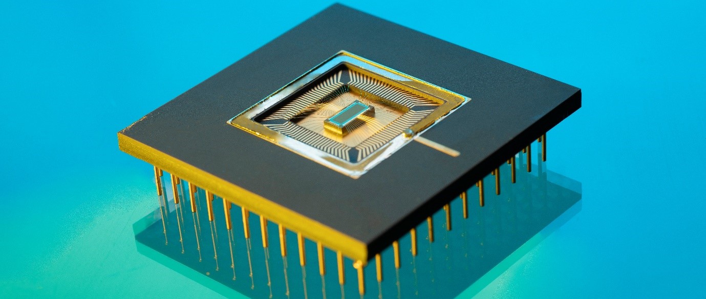
The ASIC set procured in die form according to the ESCC-Q-ST-60-05C standard for hybrid circuits was assembled into a MCCM module.
IMPLEMENTATION AND ACCEPTANCE
The wafer manufacturing was performed using a full-mask approach under the UMC180L technology. On-Wafer Acceptance Test (WAT) including Scan Electron Microscope, Electrical Die Sort, dicing and die visual inspection based on the MIL-STD-883 TM2010 standard allowed the selection of the Flight Models.
In parallel, a user-Lot Acceptance Test (user-LAT) or a qualification of the die and associated assembly process was performed by the subcontracted test house to ensure that defect allowance was acceptable to validate the reliability figures defined by the customer. Those were obtained through radiation characterization, endurance, environmental and mechanical testing.
The Radiation characterization as well as the qualification were successful. Thousands of flight models were selected from the WAT and delivered to the customer.
In 2020, a new lot including the digital and the analog ASICs was requested by Airbus for a new communications satellite.
Ready to take the leap?
Let us help you.